Parylene Coating, Parylene N, Parylene C, Parylene F, para-xylylen

Product Quick Detail
- Minimum Order
- 1
- Packaging
- N/A
- Delivery
- 2-10 Days
Specifications
Parylene Conformal Coating
Parylene is considered by many to be the ultimate conformal coating for protection of devices, components and surfaces in electronics, instrumentation, aerospace, medical and engineering industries.Parylene
- There is no liquid phase involved. Coatings are truly conformal, of uniform controllable thickness, and are completely pinhole-free at thicknesses greater than 0.5µ.
- Parylene coating
- No initiators or catalysts are involved in the polymerization, so the coating is very pure and free from trace ionic impurities.
- Room temperature formation means the coatings are effectively stress-free.
- Parylene is chemically and biologically inert and stable and make excellent barrier material.
- Parylene is unaffected by solvents, have low bulk permeability and are hydrophobic. Coatings easily pass a 100hr salt-spray test.
- Parylene has excellent electrical properties: low dielectric constant and loss with good high-frequency properties; good dielectric strength; and high bulk and surface resistance.
- Parylene has good thermal endurance: Parylene C performs in air without significant loss of physical properties for 10 years at 80°C and in the absence of oxygen to temperatures in excess of 200°C.
- Parylene is transparent and can be used to coat optical elements.
- FDA approval ofparylene-coated devices
- Parylene coatings
- Parylene coating provides an excellent barrier that exhibits a very low permeability to moisture and gases.
- Parylene coating has excellent mechanical properties, including high tensile strength.
- Parylene is stable over a very wide temperature range (-200 ‘C to +200 ‘C), allowing the chamber items coated in Parylene to be put in an autoclave.

Parylene Coating Applications
Here is a brief list of some of the items that can be parylene coated:
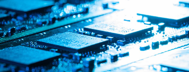
| Printed Circuit Boards | MEMs | LEDs |
| Catheters | Stents | Magnets |
| Paper | Needles | Sensors |
| Ferrite Cores | Metallic Blocks | Optical lenses |
| Implantable devices | Valves | O-rings |
| Tubing | Silicon Wafers | Keypads |
| Stoppers | Seals | Mandrels |
| Molds | Motor Assemblies | Power Supplies |
| Backplanes | Photoelectric Cells | Forceps |
| Test Tubes | Probes | Fiber Optic Components |
| Pace-makers | Bobbins | Plus Many More... |
The Parylene Deposition Process
Relatively easy to understand, theparylene deposition process
Because coating type and required surface thickness vary according to substrate material and coating-project, deposition rates fluctuate. Processing can require less than an hour or more than 24 hours, at a deposition rate of about .2/mils-per-hour. While this slower rate of substrate covering generates parylene\'s superior conformal coating, compared to other coating options, it also adds to its cost. Mastering the parylene coating process helps assure these production expenditures are diminished.
Parylene\'s complex and specialized vapor-phase deposition technique ensures the polymer can be successfully applied as a structurally continuous film, entirely conformal to the characteristics of the selected substrate. To correctly master the process, assure each incoming order possesses all pertinent information affecting parylene application. This will include drawings, specifications, and special instructions that distinguish the order from others, allowing creation of customized solutions for the particular item.
Parylene deposition
Drawn by vacuum onto the selected substrate one molecule-at-a-time in the coating chamber, the monomer gas reaches the final deposition phase, the cold trap. Here, temperatures are cooled drastically to levels sufficient to remove any residual parylene materials pulled through the coating chamber from the substrate, between -90º and -120º C.
Pre-Deposition
Mastering theparylene coating process
Thorough inspection of incoming items to-be-coated, verifying their quantity and condition. Preparation procedures enacted as necessary. For instance, cleaning/cleanliness-testing, or similar unique processes, are commenced, followed by masking of connectors and electrical components. Accumulated substrate contaminants diminish adhesion, so assuring appropriate levels of surface cleanliness is integral to parylene coating. Depending on the substrate surface, cleaning may be enacted manually, or through application of batch, inline, or ultrasonic methods. Most materials--glass, metal, plastic, etc.--require treatment with A-174 silane to effect appropriate surface modification beforeparylene application
Masking is exceptionally labor-intensive. Exceptional care is required to ensure every connector is effectively sealed, so gaseous parylene molecules do not penetrate their surfaces. All tape, or other covering materials, must thoroughly encompass the keep-out regions, without gaps, crevices or other openings, to ensure connector function is retained after coating.
Further inspection assures masking is in compliance with customers\' specifications.
The diversity of adhesion promotion methods requires a similarly diverse list of raw materials. Establishing best-adhesion practices is only part of mastering the parylene coating process; once established, strict adherence standards need to be reliably enforced to ensure quality of the conformal coatings. Using industry best practices, such as substrate cleansing and A-174 silane application, appropriately combined with standard, repeatable processes, will ensure strong adhesion for parylene coating. Adhesion promotion methods are typically used prior to the actual coating process, however some can be integrated during the process itself.
Coating Requirements
The parylene coating is applied through the deposition process described above. Once coating has been deposited, masking materials are removed; extreme caution must be exercised not to damage the thin layer of applied parylene.
An important consideration of appropriate parylene thickness is total required clearance. While an enclosure-PCB has few clearance issues, in many cases even an additional millimeter of parylene coating can be sufficient to generate dysfunctional mechanical abrasion, damaging the parylene surface and reducing its conformal qualities.
Regarding dielectric strength, items whose required levels of dielectricity are higher will need a thicker coat of parylene. Balancing dielectric strength with clearance generally requires quality testing to determine their correct ratio. The end-item customer may not always provide these specifications; learning how to determine dielectric/clearance ratios without this data is integral to mastering the parylene deposition process.
The coating process must generate a conformal covering explicitly meeting the customer\'s precise specifications. If changes are necessary, making them to order and on time are essential elements of mastering theparylene coating process
Parylene Disadvantages
The raw material,parylene dimer
Masking and otherwise prepping an article for parylene coating can be a labor intensive affair. Because parylene is applied as a vapor, it literally gets everywhere that air can. Our operators and quality inspectors must take this into account prior to coating to ensure that every one of the customer’s coating free areas are just that.
One major issue that often comes up for several of our high volume manufacturers is the limited throughput of parylene. Runs of theparylene machine
One final disadvantage of parylene to consider is the poor adhesion to many metals. Parylene has always had poor adhesion to gold, silver, stainless steel and other metals. Many printed circuit board manufacturers use gold in their products because of its conductivity. While there are some adhesion promotion methods that will greatly improve adhesion to these metals, they are either material or labor heavy and can increase costs significantly.
- Country: United States
- Business Type: Manufacturer
- Market: Americas,Asia,Europe
- Address: 213 Chestnut St.
- Contact: Sean Horn


