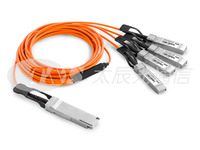
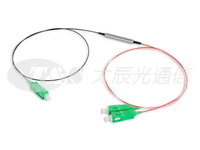
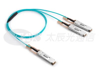
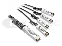
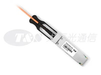
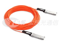
40G QSFP+BREAKOUT AOC
Specifications
T&S Communication TSQSS-8540G-xxxC is a Four-Channel, Pluggable, Parallel, Fiber-Optic QSFP+SR4 for 40 Gigabit Ethernet Applications. This transceiver is a high-performance module for
short-range multi-lane data communication and interconnect applications. It integrates four data lanes in each direction with 40 Gbps bandwidth. Each lane can operate at 10Gbps up to 300 m using
OM3 fiber. As a professional optic connector supplier in China, T&S provides china 40g qsfp to qsfp aoc cables and china 40g qsfp+ dac cables with high quality.The electrical interface uses a
38 contact edge type connector. The optical interface uses a 12 fiber MTP (MPO) connector.
Features of China 40G QSFP+Breakout AOC
Electrical interface compliant to SFF-8436 and SFF-8431
850nm VCSEL laser and PIN photo-detector
Built-in digital diagnostic functions
Operating case temperature 0℃ to 70℃
Similar to the 40G AOC produced by T&S, this AOC breakout series is also hot Pluggable
RoHS compliant
Applications of 40G QSFP+Breakout AOC
40GbE and 10GbE break-out applications for Datacom switch and router connections
40G to 4×10G density applications for Datacom and Proprietary protocol applications, Datacenters
Specifications of 40G QSFP+Breakout AOC
Absolute Maximum Ratings
Recommended Operating Conditions
Transmitter Specifications
Receiver Specifications
Parameter Symbol Min Max Unit
Storage Temperature TS -20 85 ℃
Relative Humidity RH 0 85 %
Case Operating Temperature TCase 0 70 ℃
Supply Voltage VCC -0.5 3.6 V
Pin Descriptions of 40G QSFP+Breakout AOC
Pin Definitions of 40G QSFP+Breakout AOC
Pin Symbol Name/Description
1 GND Ground
2 Tx2n Transmitter Inverted Data Input
3 Tx2p Transmitter Non-Inverted Data Input
4 GND Ground
5 Tx4n Transmitter Inverted Data Input
6 Tx4p Transmitter Non-Inverted Data Input
7 GND Ground
8 ModSelL Module Select
9 ResetL Module Reset
10 Vcc Rx +3.3 V Power supply receiver
11 SCL 2-wire serial interface clock
12 SDA 2-wire serial interface data
13 GND Ground
14 Rx3p Receiver Non-Inverted Data Output
15 Rx3n Receiver Inverted Data Output
16 GND Ground
17 Rx1p Receiver Non-Inverted Data Output
18 Rx1n Receiver Inverted Data Output
19 GND Ground
20 GND Ground
21 Rx2n Receiver Inverted Data Output
22 Rx2p Receiver Non-Inverted Data Output
23 GND Ground
24 Rx4n Receiver Inverted Data Output
25 Rx4p Receiver Non-Inverted Data Output
26 GND Ground
27 ModPrsL Module Present
28 IntL Interrupt
29 Vcc Tx +3.3 V Power supply transmitter
30 Vcc1 +3.3 V Power Supply
31 LPMode Low Power Mode
32 GND Ground
33 Tx3p Transmitter Non-Inverted Data Input
34 Tx3n Transmitter Inverted Data Input
35 GND Ground
36 Tx1p Transmitter Non-Inverted Data Input
37 Tx1n Transmitter Inverted Data Input
38 GND Ground
Pin Descriptions of 40G QSFP+Breakout AOC
Pin Definitions of 40G QSFP+Breakout AOC
PIN Symbol Name/Description
1 VeeT Transmitter Signal Ground
2 TX_FAULT Transmitter Fault (LVTTL-O) – Not used. Grounded inside the module
3 TX_DISABLE Transmitter Disable (LVTTL-I) – High or open disables the transmitter
4 SDA Two Wire Serial Interface Data Line (LVCMOS – I/O)
(same as MOD-DEF2 in INF-8074)
5 SCL Two Wire Serial Interface Clock Line (LVCMOS – I/O)
(same as MOD-DEF1 in INF-8074)
6 MOD_ABS Module Absent (Output), connected to VeeT or VeeR in the module
7 RS0 Rate Select 0 - Not used, Presents high input impedance.
8 RX_LOS Receiver Loss of Signal (LVTTL-O)
9 RS1 Rate Select 1 - Not used, Presents high input impedance.
10 VeeR Receiver Signal Ground
11 VeeR Receiver Signal Ground
12 RD- Receiver Data Out Inverted (CML-O)
13 RD+ Receiver Data Out (CML-O)
14 VeeR Receiver Signal Ground
15 VccR Receiver Power + 3.3 V
16 VccT Transmitter Power + 3.3 V
17 VeeT Transmitter Signal Ground
18 TD+ Transmitter Data In (CML-I)
19 TD- Transmitter Data In Inverted (CML-I)
20 VeeT Transmitter Signal Ground
Mechanical Specifications of 40G QSFP+Breakout AOC.
- Country: China (Mainland)
- Business Type: Manufacturer
- Market: Africa,Americas
- Address: 8 Jinxiu Middle Road, Pingshan, Shenzhen, Guangdong, China
- Contact: T&S .com

