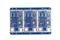
2 Layer Taconic ENIG PCB
Product Quick Detail
- FOB Price
- USD $10.00 / Piece
- Minimum Order
- 1
- Place Of Origin
- china
- Packaging
- N/A
- Delivery
- 15 Days
Specifications
Number of layers: 2
Surface finish: ENIG
Base material: Taconic TLY-5A
Min. hole diameter: 0.3mm
Outer Layer W: 1.046mil
Outer layer S: /mil
Thickness: 0.94mm
Advantages Of 2 Layer Taconic PCB
Own lamination process to convenient production for Multilayer PCB and shorten the lead time.
Jiangxi facility is environmental-friendly approved by the government .
Famous raw materials brand, Kingboard, Shengyi, ITEQ, Taiyo, Guangxin.
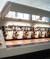
Highly automated production line with AIO Optical Scanning, Electroplating Automatic Line, High-speed flying probe test machines and inkjet printer.
Engineers with more than 15 years of experience
The management level is highly educated, 30% have professional titles and more than ten years of work experience.
High staff stability, low mobility.
UL/ISO9001/SGS/IATF16949/ROHS/ISO1400 certificated.
Sales office in Shenzhen and own 12,000sqm factory in Jiangxi.
Establish an e-commerce system to reduce transaction costs and increase market response speed.
As a professional circuit board factory, we provide bare printed circuit board, bare pcb board, bare pcb and etc. For types of pcb board or more information, please feel free to contact us!
- Country: China (Mainland)
- Business Type: Manufacturer
- Founded Year: 2017
- Address: Building 2, Xinda Park, Lvyuan Road, Xinfeng County, Ganzhou 341600, Jiangxi
- Contact: Huihe Circuits


