Blind Buried Vias & Hdi Pcb

Minimum Order
1
Packaging
N/A
Delivery
15 Days
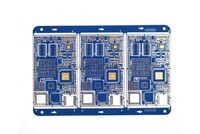
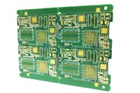
Buried vias PCB & blind vias PCB, use micro blind vias to increase the trace distribution density. Improve radio frequency, electromagnetic wave interference and hear conduction. Apply to computer server, mobile phone and digital camera products.HUIHE CIRCUITS is China HDI PCB manufacturer, Our blind buried via PCB has passed ISO9001/ISO13485/IATF16949/UL/RoHS/REACH certification.

HDI Printed Circuit Boards & Blind Buried Via PCB List

10 Layer ENIG Blind Vias PCB
12 Layer ENIG PCB
14 Layer Blind Buried Via PCB
4 Layer ENIG Blind Buried Via PCB
6 Layer ENIG Blind Vias PCB
6 Layer HASL Blind Buried Via PCB
8 Layer ENIG Blind Buried Via printed circuit board manufacturers
8 Layer ENIG Blind Buried Via PCB

Are PCB Boards With Blind And Buried Vias Called HDI PCB?

HDI circuit boards are high density interconnect PCB. The high density PCB that are plated with blind holes and then laminated are all HDI boards, which are divided into first-order, second-order, third-order, fourth-order, and fifth-order HDI. Simple buried vias are not necessarily HDI. .

The Difference Between hdi printed circuit boards And Ordinary PCB

Through Hole Circuit Board
Plating Through hole, or PTH for short, is the most common one. You only need to pick up the PCB and face the light, and the hole that can see the bright light is the "through hole". This is also the simplest type of hole, because when making it, you only need to use a drill or a laser to directly drill the through hole PCB. The cost is relatively cheap, but sometimes it will use more PCB space.
Blind Vias Hole
Blind via in PCB connects the outermost circuit of the PCB with the adjacent inner layer with electroplated holes. Because the opposite side cannot be seen, it is called "blind through". This manufacturing method requires special attention to the depth of the drilling (Z axis) to be just right; it is also possible to drill holes in the circuit layers that need to be connected in the individual circuit layers in advance, and then glue them together.
Buried Vias PCB
Buried hole, the connection of any circuit layer inside the PCB but not conducting to the outer layer. This process cannot be achieved by drilling after bonding. It must be drilled on the individual circuit layers. After the inner layer is partially bonded, it must be electroplated before it can be fully bonded. Compared with the original "through hole" and "Blind holes" take more time, so the price is the most expensive. This process is usually only used for high density interconnect PCB to increase the usable space of different types of PCB board layers.

Huihe Circuits is a professional printed circuit board maker and hdi pcb factory, we provide blind via in pcb, high density interconnect pcb, hdi pcb china, blind buried via pcb, pcb boards for sale and etc. For hdi pcb price or more information, please feel free to contact us!

  • Country: China (Mainland)
  • Business Type: Manufacturer
  • Market:
  • Founded Year:2017
  • Address:Building 2, Xinda Park, Lvyuan Road, Xinfeng County, Ganzhou 341600, Jiangxi
  • Contact:Huihe Circuits
*Your name:
*Your Email:
*To:Xinfeng Huihe Circuits Co., Ltd.
*Subject:
*Message:
Enter between 20 to 3,000 characters. English only.     Characters : 0 / 3000
*Enter the secure code shown below Mfrbee security Image      Reload Image

submiting now We do inquire for you , please wait ...

6 Layer HASL Blind Buried Via PCB

Number of layers: 6 Surface finish: HASL Base material: FR4 Outer Layer W/S: 9/4mil Inner layer W/S: 11/7mil Thickness:1.6mm Min. hole diameter: 0.3mm Special process: Blind Vias Advantages Of 6 Layer HASL Blind Buried Via PCB Own lamination process to convenient production for ...

Xinfeng Huihe Circuits Co., Ltd.

14 Layer Blind Buried Via PCB

Number of layers: 14 Surface finish: ENIG Base material: FR4 Outer Layer W/S: 4/5mil Inner layer W/S: 4/3.5mil Thickness: 1.6mm Min. hole diameter: 0.2mm Special process: Blind & Buried Vias Advantages Of 14 Layer PCB Own lamination process to convenient production for ...

Xinfeng Huihe Circuits Co., Ltd.

10 Layer ENIG Blind Vias PCB

Number of layers: 10 Surface finish: ENIG Base material: FR4 W/S: 4/4mil Thickness: 1.6mm Min. hole diameter: 0.2mm Special process: Blind Vias Advantages Of 10 Layer ENIG Blind Vias PCB Own lamination process to convenient production for Multilayer PCB and shorten the lead ...

Xinfeng Huihe Circuits Co., Ltd.

HDI 3mil control panels PCB in Consumer electronics with  impedance control blind and buried holes
HDI 3mil control panels PCB in Consumer electronics with impedance control blind and buried holes

HDI 3mil control panels PCB in Consumer electronics with impedance control blind and buried holes Application Field: Consumer electronics Layer/Board Thickness: 12L/1.6mm Surface Treatment: ENIG Line/Space: 4/4mil Smallest Hole Diameter:0.15mm Technical Feature: impedance ...

HX Circuit Technology Co.,Ltd.

Controlled Impedance 6L/1.6mm HDI PCB in Mobile with blind and buried holes

Application Field: Mobile Layer/Board Thickness:6L/1.6mm Surface Treatment: ENIG+OSP Line/Space: 3.5/3.5mil Smallest Hole Diameter:0.15mm Technical Feature: 1+4+1, impedance control blind and buried holes HX’s capacity ranges from prototype to production volume’s with our ...

HX Circuit Technology Co.,Ltd.

blind and buried holes HDI PCB equipment manufacturers with tablet computer 10:1 Aspect ratio

blind and buried holes HDI PCB equipment manufacturers with tablet computer 10:1 Aspect ratio Application Field: tablet computer Layer/Board Thickness: 8L/1.6mm Surface Treatment: ENIG Line/Space: 3/3mil Smallest Hole Diameter:0.1mm Technical Feature: 1+6+1, blind and buried ...

HX Circuit Technology Co.,Ltd.

Printed Circuit Board With Blind And Buried Vias

Shenzhen Hejin Circuit Co.,Ltd is a leading printed circuit board with blind and buried vias exporter, and one of the leading China printed circuit board with blind and buried vias manufacturers, producers and suppliers. We export high quality products, and we are professional ...

Shenzhen Hejin Circuit Ltd.,Co.

PCB With Blind And Buried Vias

Shenzhen Hejin Circuit Co.,Ltd is a leading PCB with blind and buried vias exporter, and one of the leading China PCB with blind and buried vias manufacturers, producers and suppliers. We export high quality products, and we are professional at PCB with blind and buried vias ...

Shenzhen Hejin Circuit Ltd.,Co.

Medical Control Buried And Blind HDI Multilayer PCB High Density PCB

Place of Origin: SZ,GD,China Manufacturer: Rigao Electronics Services Code: RG-002 Product Name: Medical Control Buried and Blind HDI multilayer PCB High Density PCB Board material: FR4 Board thickness: 1.2mm PCB Layers: 12 layers Copper thickness: 1oz Surface finishing: ENIG ...

Shenzhen Rigao Electronics Co.,Ltd