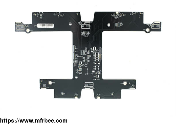
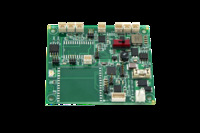
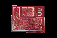
Fastlink Electronics Through Hole PCB Assembly Supplier
Specifications
Our DIP process workers are rich experienced with a variety of products. They can solder them very beautifully.
Through hole assembly is used in many fields. The time and money required to complete an through hole mount PCB Assembly makes it especially popular for large equipment applications such as
transformers, semiconductors and electrolytic capacitors.
Also because of its characteristics, it can provide sufficient safety for those equipment that must withstand high levels of mechanical or environmental pressure as well as high power and high
pressure conditions.
Through hole pcb assembly supplier Fastlink Electronics has invested in the most advanced welding and assembly tools available on the market today with the aim of providing better service to our
diverse customer base, choosing us is choosing success.
What Are The Applications For Through-hole PCB Assembly?
Through-Hole PCB Assemblies are widely used in military and aerospace products for extreme acceleration, collision, or high temperatures. Because of pcb manufacturing and assembly ability to
withstand higher environmental stresses, they are suitable for high-reliability products requiring stronger interlayer bonding.
In addition, through-hole PCB Assemblies are used in testing and prototyping applications, especially for products that require manual adjustments and replacement of components.
Through Hole Pcb Assembly Design Process
The through-hole PCB fabrication and assembly design process involves several steps to ensure proper component placement and secure soldering. When working with a reliable service provider like
Fastlink Electronics in China, the following steps are typically followed:
Component Placement: The first step is to determine the optimal placement of through-hole components on the PCB. This includes selecting appropriate footprints and considering factors such as
component height and spacing.
Drilling and Plating: After component placement, holes are drilled in the PCB at designated locations. The holes are then plated to ensure proper electrical conductivity and connection between
layers.
Component Insertion: Through-hole components are inserted into the pre-drilled holes on the PCB. The leads of the components extend through the board.
Wave Soldering: The PCB is passed through a wave soldering machine, where a wave of molten solder is used to solder the through-hole components. The solder forms strong electrical and mechanical
connections between the component leads and the PCB.
Inspection and Testing: The assembled PCB undergoes thorough inspection and testing to ensure proper solder joints, component alignment, and electrical connectivity. Any issues or defects are
identified and addressed during this stage.
Cleaning and Finishing: After successful inspection, the PCB is cleaned to remove any flux residue or contaminants. It is then finished with any necessary coatings or protective layers.
Surface mount through hole PCB assembly is commonly used for components that require high mechanical strength or when hand soldering is preferred. Fastlink Electronics, as a reputable electronics
manufacturer in China, has expertise in through-hole PCB assembly, ensuring precise component placement and reliable soldering for optimal product performance.
PCA printed circuit assembly
HOW DOES THROUGH HOLE PCB ASSEMBLY WORK?
Step 1
The hole and pad to be soldered are prepared, with the lead being placed into/through the hole. The lead should be placed in such a way as to keep the bend above the soldered area to reduce heat
and solder requirements.
Step 2
Heat is applied evenly to the lead and the pad/hole, heating the material so the solder will adhere to both surfaces.
Step 3
The solder contacts the end of the iron, which leads the solder to change into a liquid and flow into the hole.
Step 4
The solder flows through the hole, creating a mound on both the bottom and topside. Since this lead was soldered from the top side, the bottom side should be inspected for adequate solder and joint
quality. Some assembly may require solder from both sides to ensure quality. Adequate clearance inside the hole allows good solder flow through the board, allowing only one side to have solder
applied. Tight clearances may require soldering on both sides, increasing soldering time.
As the best chinese pcb manufacturer, we can offer sorts of related products for sale, if you have needs, please contact us.
- Country: China (Mainland)
- Business Type: Manufacturer
- Founded Year: 2009
- Address: A310, HuaFeng Bussiness Building, Xixiang Rd, Bao'an, ShenZhen
- Contact: fastlink electronics
