PCB Surface
Specifications
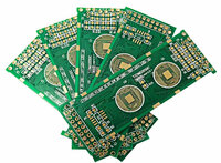
PCB surface finish include: surface PCB finish is a coating between a component and a bare board PCB. It is applied for two basic reasons: to ensure solderability, and to protect exposed copper
circuitry. As there are many types of surface pcb plating finishes, selecting the right one is no easy task, especially as surface mounts have become more complex and regulations such as RoHS and
WEEE have changed industry standards.
Recently, the common PCB surface treatment technologies which GreensTone may use when manufacturing PCBs are HASL(hot air solder leveling), organic coating (OSP), electroless nickel/gold, immersion
silver, immersion gold, etc.
The solder mask is mainly Liquid UV Photo-imageable Ink with green, red, black, yellow, white, matt black/green, bule, gray, etc. green should be the most commonly used one. The suggested
soldermask clearance in GERBER is 2-4 mils.
The silkscreen layer is the top layer of the PCB and serves as a reference indicator for placing components on the PCB. The graphics and text on PCB, a circuit board is usually printed with a
permanent non-conductive epoxy ink. The color is typically white. Screen printing is used to specify useful information on the PCB board, which can help users during the assembly. It is used to
mark component values, part numbers, test points, polarity, etc.
PCB Surface Features
PCB finish Comparison of cost and solderability
Actual solderability: Electroplating nickel gold> HASL > OSP > ENIG >Immersion silver >Immersion tin
Cost: Electroplating nickel gold > ENIG > Immersion silver> Immersion tin > HASL > OSP.
The functions of the solder mask layer on the SMT PCB board
Preventing short circuit from bridge connection in the soldering process
Preventing the physical breakage of a conductor circuit
Prevent short circuit between conductive lines and solder joints when proceeding reflow soldering, wave soldering, and manual welding
Preventing the copper layer from oxidation
Its high Insulating brings the possibility to the high density of PCB boards
Here are three main ways to add silkscreen coating on a PCB
Manual screen-printing: This is a process that can be used when line widths are greater than 7 mm and the registration tolerance is 5 mm.
Liquid Photo Imaging (LPI): This process provides more accuracy and legibility over manual screening and is used when line widths are greater than 4 mm
Direct Legend Printing (DLP): This is the most accurate way of adding a silkscreen, however, it is very expensive.
PCB Surface Manufacturing Introduction
HASL (hot air solder leveling)/HASL lead Free HASL/HASL lead free is the process of coating tin-lead/ tin-lead free solder on the surface of PCB so that it forms a layer of both anti-copper
oxidation and good weld ability of the coating.
Organic Coating (OSP) OSP is a chemical process to build a layer of organic skin film on the clean bare copper surface, it helps anti-oxidation,and moisture resistance, to protect the copper
surface from vulcanization or oxidation, etc. In simply words,OSP acts as a barrier between copper and air.
ENIG (Electroless Nickel/Immersion Gold) ENIG is a thick nickel gold alloy with good electrical properties on the copper surface,acts as a rust barrier to protect PCB for a long time, which can be
useful and achieve excellent electrical performance in the long term use of PCB.
Immersion Silver Silver impregnation does not put heavy coat on PCB, which provides good electrical properties and maintains good solder ability when exposed to humidity ,heat,and pollution,
Immersion Tin With adding organic additives to the tin layer, the tin layer structure is granular, which overcomes the tin whisker problems and has excellent thermal stability and solder ability.
If you are looking for a reliable ems manufacturing company, please choose us, and we will be your best partner.
- Country: China (Mainland)
- Founded Year: 2011
- Contact: green pcba
