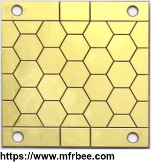
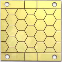
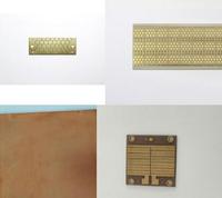
Sliton Single & Double-sided Ceramic PCB
Specifications
With the development of high technology, people need electronic products with high performance, small volume and many
functions.Therefore,the PCB manufacturing is also developedinto the direction of
beinglighter, thinner, shorterand smallerwith limited space, more functions,
greater wiring density and smaller aperture.From 1995 to 2005, the minimum pore size of mechanical drilling capacity decreased from 0.4mm to 0.2mmandeven
smaller.The size of metallized pore is also getting smaller and smaller.The quality of metallized holes dependingon the interconnection
betweeneachlayer is directly related to the reliability of PCB.
The double-sided ceramic PCB board is an important PCB board in the circuit board. Therearedouble-sided ceramic PCB boardofPCB metal
base, Hi-Tg heavy copper foil circuit board, flat&winding double-sided circuit board, high-frequency ceramic PCB, high-frequency double-sided circuit
boardofhybrid dielectric base, etc.in the market.It isapplicable for a wide range of high-tech industries such as
telecommunications, power supply, computer, industrial control, digital products, scientific and educational instruments, medical devices, automobiles, aerospace
defense,etc.
The difference between the double-sided ceramic PCB board and the single-sided ceramic PCB board is that the single-sided ceramic PCB circuit is only on one side of the ceramic PCB board,
while the double-sided ceramic PCB circuit can be connected through holes in the two sides of the ceramic PCB board.The parametersand
fabricationof double-sided ceramic PCB platemakeitdifferent fromsingle-sided ceramic PCB plate.Besides the process of
making, there is also a copper sinking process, which is the process of conducting the double-sidedwires.
Sliton’ssingle&double-sidedceramic PCB, asthe best ceramic PCB in China, can use laser technology to achieve the perfect combination of ceramic and copper layers with the10%increase ofoverall performance.Besides single&double-sidedceramic PCB,theboxdamPCB,special-shaped ceramicPCB, andmultilayer ceramicPCB top thedomesticmarket.
1.Substrate type:aluminium nitride ceramics
Substrate material thickness:0.65mm
Conducting layer:Cu
Thickness of metal layer:75μm/75μm
Surface preparation:immersion gold
Metal single-sided / double sided:double sided
Copper plated through hole:yes
Solder mask:no
- Contact: pengliang Tu


