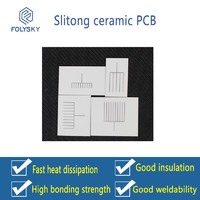
Ceramic substrate for optical communication


Product Quick Detail
- Place Of Origin
- china
- Minimum Order
- 1
- Packaging
- N/A
- Delivery
- 15 Days
Specifications
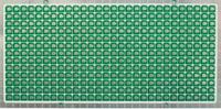
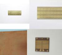
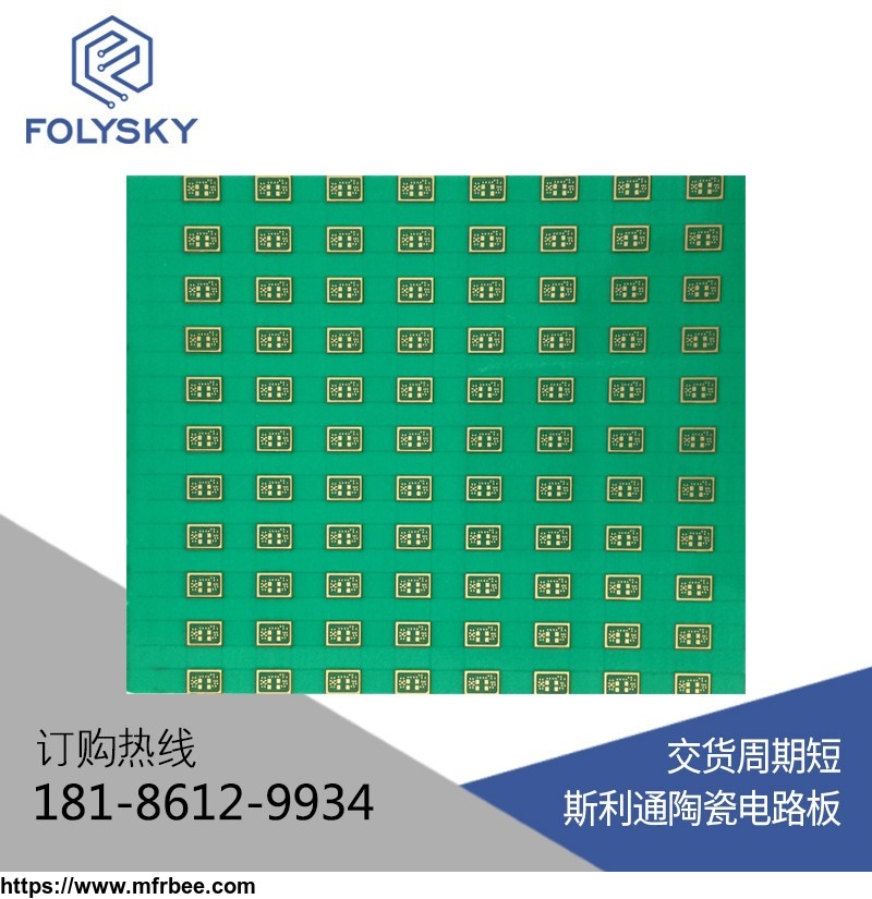
Product introduction
Substrate material thickness:0.38mm
Conducting layer:Cu
Thickness of metal layer:100μm/35μm
Surface preparation:immersion gold
Metal single-sided / double sided:double sided
Copper plated through hole:yes
Solder mask:yes
Product features:
The ceramic circuit board has high accuracy and good electrical and thermal properties
2. ceramic circuit board with high bonding strength and good weldability, can realize blind through hole
3. ceramic circuit board technology is mature, environmental protection, pollution-free, cost is lower than traditional technology
4., a wide range of applications, single-sided and double-sided three-dimensional ceramic circuit boards can be produced
5. customized production, without mold opening, short production cycle
6., no organic ingredients, resistant to cosmic radiation, high reliability in aviation and space, long service life.
7. can carry out high-density assembly, line / pitch (L/S) resolution can reach 20 m, so as to realize the integration and miniaturization of equipment.
8. high frequency loss, it can be used in high frequency circuit.
9. copper sealing, high reliability.
10. 3D substrate and 3D routing.
- Contact: pengliang Tu